Thursday, December 31, 2015

Inside the armv1 Register Bank - register selection

In an earlier post I reverse engineered the register bank, but stopped once I had identified the b3..b0 inputs for each of the 3 sets of register select logic. This information was summarised in a table which I've copied below:

Now that we have identified the Instruction Register it becomes practical to identify how these signals are derived.

Let's start with Read Bus B, bit 3:


This circuit is a 5 way input multiplexer (there are many similarities to the Read Bus Decoding logic we found earlier). The 5x AND gates forming the selection logic feed the multiplexer logic for all 4 bits.

The result, which includes all 4 bits can be summarised in the table below:

So the various PLA-2 outputs between them select whether Read Bus B has r14 (probably for the Branch and Link instruction), one of 3 different bit-regions of the currently executing instruction, or the output of the priority encoder. This last option will be for the LDM/STM load/store multiple registers instruction.

Read Bus A is also fed from a 5 way input multiplexer, but the selection logic is much simpler:


Two of the multiplexer "channels" comprise N-FETs (those driven by the inverters in the circuit above), with the and remaining "channels" constructed of P-FETs, The multiplexing operation across all 4 bits is:


The Write Bus is fed from a 5 way input multiplexer too, with the following circuit:

The results of it's multiplexing across all 4 bits is:

 Let's drill down on the priority-encoder signals.


So the 4 bit wide priority-encoder signal is delayed slightly before being used as input the Read Bus A multiplexer and Write Bus multiplexer. The circuit for the remaining 3 of the 4 bits is identical.

Conclusion

This analysis has significantly clarified our understanding of how the registers selection works - the PLA-2 outputs control which fields from the Instruction Register are used to select the 3x register bank inputs/outputs. There are a few exceptions where r14 or r15 is selected or the data from the priority encoder is used.

Only approximately 150 transistors are used to implement these circuits.

Wednesday, December 30, 2015

Inside the armv1 Read Bus

Having explored the Register Bank last time, a good next step is to explore where its two read port outputs go. In this blog we'll start with Read Bus B, as that will also lead us the Data Bus and the data line pins. As a reminder from my earlier blogs, the floorplan is in the following diagram although, as we will see, there are several detailed differences in the actual chip. Also remember, as pointed out in the last blog, this diagram incorrectly swaps the read bus A and read bus B.


This exploration will end up covering a lot of ground - we'll find the Instruction Register and the instruction bus that feeds off it, and how data is routed in and out of the chip via the data bus. The diagram below highlights the areas of the chip we'll end up exploring.


To help navigate our way around the more complex logic, I've labelled the different areas in a zoomed in area of the top of the larger rectangle.


The logic for each bit associated with the Read Data Bus is laid out horizontally, and with the bits stacked on top of each other vertically - bit 31 at the top, and bit 0 at the bottom. Read Data Bus bit 31 is highlighted in red, and the areas labelled 1, 2, 3, 4 highlight the logic gates associated with bit 31. The logic is almost identical for all 32 bits, and the associated drive circuitry highlighted at the top. Also highlighted as area 5 is the logic associated with one of the data pins; we'll reverse-engineer that logic too.

We'll start by following where bit 0 of Read Bus B leads us, and then see how the remaining bits of the bus differ.


This circuit relies on stray capacitance on the bus line for its operation. During the second half of every clock cycle (when phi 2 is high) the FET in the above circuit pulls the bus line high, charging it to a high state. In the subsequent first half of the next cycle, one of three possible signals may pull the bus line low, discharging any stray capacitance. The state of the bus line is then read by either the Barrel Shifter or by Circuit 4, which processes the Data Out signal. The signal on the Read Bus is inverted logic - 0v represents a logical 1.

The signal input to the bus is one of the following:
  1. The output of the Read Bus B from the Register Bank, as described in the last blog.
  2. Data from Circuit 1, which is described below, and can be either the content of the Instruction Register, or data from the Data pins.
  3. Data for when the PC is being read. The armv1 architecture is such that the program counter (PC, which is R15 in the register bank), has special meanings assigned to some of its bits. These bits are not stored in the register bank, but elsewhere. Bits b0..b1 give the processor state, and bits b26..b31 are the Condition Code Register. The logic above is to read these registers at the appropriate time. This data path is in the thin vertical rectangle in the diagram above. This logic will be explored in a later post.
Complexity arises with how the circuit differs for each bit. We've already dealt with how input 3 varies. However the enable (8106) for the data from Circuit 1 also varies in a complex way. There are 5 (!) enable lines across all 32 bits of Read Bus A:


One use of this circuitry is for when a byte-read takes place - the 8 bits of data just read appear on different bit ranges depending on the lower two address bits. The enable signals above allow the valid data to put onto the Read Bus (the barrel shifter then rotates the bits to the correct position). I don't yet understand why the second and third enable signals drive just 4 bits each. The circuitry to create these 5x enable signals is in the DATA CTL area - the red rectangle at the top right of the chip:


As can be seen from the diagram, each enable output is dependent on the result of a 4:1 multiplexer. Each multiplexer has 3 of its 4 inputs that are hardwired to either a 0 or 1. The fourth multiplexer input is dependent on additional logic, including the bw output pin. The bw output pin indicates whether the current memory read/write operation is for a byte transfer or a 32 bit word transfer (high for word, low for byte). The truth table below is another way to see the operation.


The top three rows demonstrate that the first three inputs (phi 1 clock, 8186, and 8272) must have values 1, 1, 0 respectively for there to be any output. The next three lines show the outputs for three of the possible permutations of 8105, 8104. I suspect that these are for instruction decoding:
  • the first to extract the 8 bit immediate value for one variant of the Data Processing instruction.
  • the second to extract the 12 bit offset for the Single Data Transfer instruction.
  • the third to extract the 24 bit offset for Branch instructions.

The next 4 rows in the table are to select each byte in turn. It's almost certain 8195, 8194 are connected to Address line 1, 0.

Circuit 1 - Data In and I-Reg Multiplexing

Now that we have the circuit for the enable signal for Circuit 1 let's look at Circuit 1's internal logic, and its associated driver circuit.


So this circuit puts either Data In or I-Reg onto Read Bus B, depending on two control signal from elsewhere - signal 8111 or 8187.

The back-coupled FETs that signal 8111 feeds into warrants a little more discussion. This back-coupled FET pattern is used in many places throughout the processor, including in the ALU. This pattern appears to have two distinct uses:

  • It can be used ax a multiplexer, as shown further down in the same circuit. 
  • Or in this case it can be used as a "latch". Whilst the phi 1 clock is high both FETs are turned on and the 8111 signal passes through the FETs to the input to the AND gate. When the phi 1 clock goes low the two FETs are turned off and the input to the AND is left floating. The stray capacitance of the node means the voltage will be maintained for a short period, until any charge is dissipated through leakage. The capacitance must be large enough, and the leakage small enough, for the correct logic value to be maintained until the next clock cycle. This is presumably why the processor has a maximum clock cycle time of around 10 microseconds; any longer and the correct value would not be held.
So, in summary, signal 8111 is "latched" during the phi 1 clock time so that it can be processed during the phi 2 clock time.


Circuit 2 & 3  - The Instruction Register (or I-Reg)

The Instruction -Register logic is as follows:


The Instruction Register itself is the cross-coupled inverter on the right, although it's difficult to see with the FET multiplexers at each inverter's input. The pair of multiplexers that feed the lower cross-coupled inverter determine whether the register maintains its current (looped back) state or whether it is updated from a delayed copy of Read D0. Input 8187 selects which multiplexer is selected. The 3x input signals that control this circuit will be explored subsequently, but a quick look shows that input 4585 is derived from the opc pin, which indicates that the processor is fetching an instruction, so we're definitely on the right track!

The I-Reg outputs form a bus that runs right across the chip, pretty much as illustrated in the floorplan at the beginning of this blog. However, there are a few exceptions:

  • A few outputs are not connected. These are bits 25, 26, and 27.
  • There are 6x I-Register outputs that are fed from the opposite side of the cross-coupled inverters. These are bits 4 (7887), 20 (7888), 24 (7889), 25 (7890), 26 (7891), 27 (7892). These all feed into inverters and the inverted outputs join the other I-Reg signal bus. The inverters are in the area marked "3 Outputs" in the earlier image.

Circuit 4  - Data Out (DOUT) Processing

The final circuit connected to Read Bus A is the Data Out (DOUT) processing logic which in the area marked as "4" in the earlier image:


This logic interfaces the Read Bus with the processor's data bus. Normally all 32 bits of the Read Bus are presented to the data pins; however during a byte-write, the data in the lowest byte is also presented on 3 the upper bytes too.

The logic for the 8 lowest bits is the identical, and passes the signal to the other bits via an 8-bit wide bus, and also towards the Read/Write pin on nbus signals.

The logic for bits 8-31 is also identical. The signal is multiplexed in from either the Read Bus B input or from the 8-bit wide bus fed by bits 0..7. The bw (byte not word) input signal selects between the two inputs. We've already encountered the bw input signal in the Read Bus B decoding logic.

Circuit 5  - Data Lines 0 to 31

The final circuit to explore is associated with each data line, and is highlighted in the diagram above as circuit 5.


This circuit identifies the destination of the nbus signal referred to in the Data Out logic, and the source of the Read D0 signal that's seen in the Data In logic, and the Instruction Register logic.

We also see the R/W pin, and the dbe (data bus enable) pin having a part to play in the logic.

Conclusion

We have finally completed our exploration of the Read Bus B logic, and in the process identified the Instruction Register (I-Reg) and how data is read and written to the data pads. We've also seen some of the complexities of dealing with byte/word reads and writes and how reading r15 (the PC) is a special case. Around 2,200 transistors are used to implement these circuits.

To have located the Instruction Register is an important step forward as it is its content that drives much of the processor's control logic. But all that is for future blog posts.

But let's not get lost in the details. Overall, the circuitry described in this post accomplishes some simple routing, which are summarised in the diagram below, which is a little more explicit than the floorplan diagram above. Yes, there are extra details that aren't shown in the diagram, but it helps to keep this overview in mind too.


Monday, December 28, 2015

Inside the armv1 Register Bank

Reverse engineering the armv1 chip feels a lot like completing a jig saw puzzle. I start with the more obvious "chunks", and then gradually fill in the gaps that are left. A very big "chunk" on the armv1 chip just crying out to be reverse-engineered is the register bank, and that's where I'll start today before moving on to look at the main data paths.

Architectural descriptions of the armv1 tell us that the chip contains a bank of 25 registers, each 32 bits wide. Of these 25 registers, only 16 are visible to the programmer at a time and are referenced in the instructions as registers number 0 to 15, with register 15 being the Program Counter or PC. The extra registers are there to support the four modes that the processor runs in - supervisor, interrupt, fast interrupt, and user mode. For instance the fast interrupt mode has it's own copy of five of the registers - r10, r11, r12, r13, and  r14.

We also know from the architecture that the register bank has two read buses and one write bus. We also know from my last blog that one of the read buses goes directly to the ALU, and that the output of the ALU goes to the write bus. This is nicely illustrated in the following block diagram:


(Please note that it has recently been noticed that this historical diagram has incorrectly labelled read bus A and read bus B the wrong way around; all other documents name them the other way around. This blog series has therefore been updated to label the buses correctly)

Now that we have a bit more context it's time to zoom into the details on the chip, starting at the lowest level of detail - a single bit. Each of the 32 bits of all 25 registers is the same - a cross-coupled inverter, with three separate select lines. The silicon layout is as follows:

The equivalent circuit is:


What is interesting about this circuit is that the write circuit shorts the output of one of the inverters! The write select transistor and the Write Bus driver transistors are comparatively large, and much larger than the transistors in the inverter, ensuring that they will "win". Once the inverter's output has been overpowered, the cross-coupled inverters will quickly transition to the new state, ensuring that the short condition lasts only a very short time. The 3x select lines per register run vertically, as shown in the chip detail above. Likewise, the 32 bits per register (x3, one for each bus) run horizontally.

Select Line Decoding

The three select lines for each of the 25 register are generated by the decode circuitry above the register bank. The similarities in the decoding between the three select lines, and between the registers is visually very apparent:


I'll start by describing the decode circuitry for Read Bus B, and later show how the decoding for Read Bus A and the Write Bus differ only slightly. There are two steps to the decoding process, first decoding the register number, and then the processor state/mode. Decoding by the register number is via the following circuit:


I've laid out the diagram so such that the horizontal lines match the chip layout. The b3, b2, b1, b0 inputs select the register; the logic to set these values will be reverse-engineered in a later blog. Note that each input to the NAND gate has only one connection (not 2 as shown in the diagram) - it will be connected either to an input bit or its inverse.

The subsequently decoding based on processor state/mode is as follows:


Again, the diagram is laid out so that the horizontal lines match the chip layout. The C NOR input is connected to just one of the 5 horizontal lines that select the processor modes. The output of the AND gate feeds to the register array. Note that the horizontal lines also feed the Read Bus B and Write Select logic.

The settings for the 25x sets of decoders are summarised in the table below:


The decoding for the Read Bus A and Write Select is very similar. The registers selection logic is almost identical, with only the source of the b3..b0 input signals differing, as shown in the table below:


There are only minor differences in the processor state/mode decoding.The updated circuits are shown below:


Note that the write decoding is driven from the phi 2 clock, whereas both sets of read decoding is driven from the phi 1 clock. We'll  need to pick up on the timing-related aspects later.

Finally, r15, the Program Counter, has some slight variations from the above; these need to be investigated later.

Conclusion

We now have a complete breakdown of the register bank and how the three ports - two read, and one write - operate. A little over 6,000 transistors are needed for its implementation. There are very few external signals that control its operation, and these will be clarified later as we continue with the reverse engineering.


Saturday, December 19, 2015

Inside the ALU of the armv1 - the first ARM microprocessor

This is the first in a series of posts on the armv1. The full list of posts is:
Ken Shirriff has also written a series of ARM posts arm internals here.

I really enjoyed reading Ken Shirriff's blogs about reverse engineering the 8085, (e.g. Inside the ALU of the 8085 microprocessor), and immediately thought of his articles when I saw that the guys over at visual6502.org announced that they had released the mask level details and full simulation of the very first arm chip - the armv1.

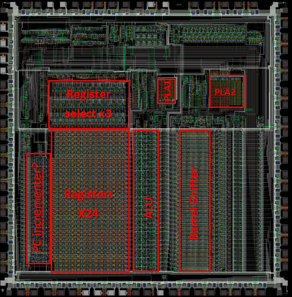
With that in mind I embarked on my own attempt to reverse-engineer parts of the armv1. Some background knowledge of the processor's architecture is helpful, and googling for "ARM Architecture Reference Manual" will lead you to very detailed descriptions of the more modern versions of the processor. By just looking at the masks and knowing a little about the processor's architecture it's possible to make some good guesses at what some of the blocks are.


The barrel shifter is especially obvious when you go to the interactive visual6502.org website and zoom in on that portion of the chip and see the diagonal traces. Also, from the architecture description, we know each data-processing (ALU or arithmetic logic unit) instruction selects 3 registers: one destination register (where the ALU result goes), and a register for each of the two operands - Operand 1 and Operand 2. It is therefore a reasonable guess that the Register file has 3 sets of register selection logic, which is verified by the 3 layers of gates of very similar pattern directly above the Register file.

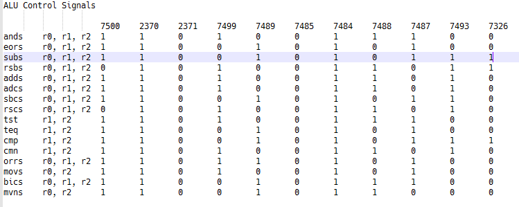
From the architecture description we know that ALU is controlled by 16x opcodes:


So my first step was to ensure I'd found the right area for the ALU. From the architecture description I know that the two inputs to the ALU are:
  • Operand 1: the content of register n, as selected by the Rn field of the instruction.
  • Operand 2: the output of the barrel shifter (most operations select a shift of 0).
I therefore started by reverse-engineering the barrel-shifter and identifying the barrel-shifter's output. By following the output I knew it would lead to the ALU.

The steps I took to reverse-engineer the ALU were to identify each of the transistors and how they are connected (using the netlists on the visual6502.org website), converting these into gate circuits, translating these into a schematic, and finally verifying I had captured it correctly by cross checking the simulator's output against the circuit in the schematic.

The portion of the die associated with a single bit slice of the ALU is here:


An example of the translation of transistors into a gate (which corresponds to the upper left circuit of the ALU) is as follows:


The full ALU circuit contains 70+ transistors for each of the 32 bits, or over 2,200 transistors in total.


This diagram corresponds to a single bit in the ALU, so this is replicated 32 times to form the full ALU. On the physical silicon these are stacked one on top of the other, although physically the circuit is swapped left for right, as the inputs to the ALU are from the right-hand-side and exit on the left-hand-side.

In the schematic above the control signals (7500, 2370, etc. - these are their net numbers) are shown coming into the circuit from above and below; on the physical silicon all these control signals originate from above the ALU.

The eagle-eyed will also notice that the Carry propagation and Zero calculation circuits alternates slightly between each bit, with b0, b2, etc identical, and b1, b3, etc. identical. The end result is the same but the reason for the difference is to keep the execution path as fast as possible by eliminating an inverter per bit; note that the Carry Out and Zero Out signals are opposite polarity to the inputs.

The 16x different ALU operations are selected by the appropriate setting of the control signals as shown in the table below.


The schematic and the table above give a huge amount of detail! However it can be broken down into smaller, more digestible pieces.

First, note that 2370, 2371, 7484, and 7485 all have the same setting for each opcode; they, and the associated FET transistor isolation circuitry, can be ignored (their purpose is for another discussion).

Second, note that 7393 is only high when it's an arithmetic operation - it purpose is to enable/disable the Carry chain.

Third, Control signal 7500, and the 3x gates at the top left of the schematic, determine whether Operand 1 is inverted on entry to the rest of the ALU (note that the input signal is already inverted, so the 'normal' setting is for it to be 1 to invert it again).

Fourth, control signals 7489 and 7499 select whether Op 2, or its inverted version, is selected through the upper path and to point (A) marked on the schematic.

Similarly, control signals 7487 and 7488 select whether Op 2, or its inverted version, is selected through the lower path and generates signal (B) on the schematic.

The instructions that require a subtraction  - sub (subtract), rsb (reverse subtract), and cmp (compare) - do so by converting the associated operand into its twos-complement form by inverting all the bits and adding 1 by feeding a '1' into bit 0 of the carry chain (7326) and then performing an add operation.

The various logic operations (and, or, exclusive or, and bit clear) are selected by selecting the appropriate polarity of each input operand and choosing the right combination of 7489, 7499 and 7487, 7488. For example, note that the only difference in the control signals between the 'and' opcode and 'bic' opcode (bit clear), is that the values on 7489 and 7499 are swapped causing the inverted form of Operand 2 to be fed into the upper calculation path. This is while both 7487 and 7488 are forced high causing signal (B) to be low irrespective of the input.

The table below shows for all of the opcodes some of the intermediate results, and the outputs for one combination of input bits.


So how are the control signals generated? They're created by PLA-1, but how that part of the circuit works is for another day.